Electron microscopy has allowed scientists to see individual atoms, but even at that resolution not everything is clear.
The lenses of electron microscopes have intrinsic imperfections known as aberrations, and special aberration correctors – “like eye glasses for your microscope,” said David Muller, the Samuel B. Eckert Professor of Engineering in the Department of Applied and Engineering Physics (AEP) – have been developed over the years to correct these defects.
Aberration correctors only go so far, however, and to correct multiple aberrations, you need an ever-expanding collector of corrector elements. It’s like putting glasses on glasses on glasses – it becomes a bit unwieldy.
Muller – along with Sol Gruner, the John L. Wetherill Professor of Physics, and Veit Elser, professor of physics – have developed a method for achieving ultra-high resolution without the need for “corrective lenses” for their microscope.
They’ve employed their Cornell-developed electron microscope pixel array detector (EMPAD), which was introduced in March 2017. With it they’ve achieved what Muller, co-director of the Kavli Institute at Cornell for Nanoscale Science, said is a world record for image resolution – in this case using monolayer (one-atom-thick) molybdenum disulfide (MoS2).
Their achievement is reported in “Electron Ptychography of 2D Materials to Deep Sub-Ångström Resolution,” to be published July 19 in Nature. Co-lead authors were Yi Jiang, Ph.D. ’18 (physics) and Zhen Chen, postdoctoral researcher in the Muller Group.
Electron wavelengths are many times smaller than those of visible light, but electron microscope lenses are not commensurately precise.
Typically, Muller said, the resolution of an electron microscope is dependent in large part on the numerical aperture of the lens. In a basic camera, numerical aperture is the reciprocal of the “f-number” – the smaller the number, the better the resolution.
In a good camera, the lowest f-number or “f-stop” might be a little under 2, but “an electron microscope has an f-number of about 100,” Muller said. Aberration correctors can bring that number down to about 40, he said – still not great.
Image resolution in electron microscopy has traditionally been improved by increasing both the numerical aperture of the lens and the energy of the electron beam, which does for the microscope what light does for a camera or an optical microscope – illuminates the subject.
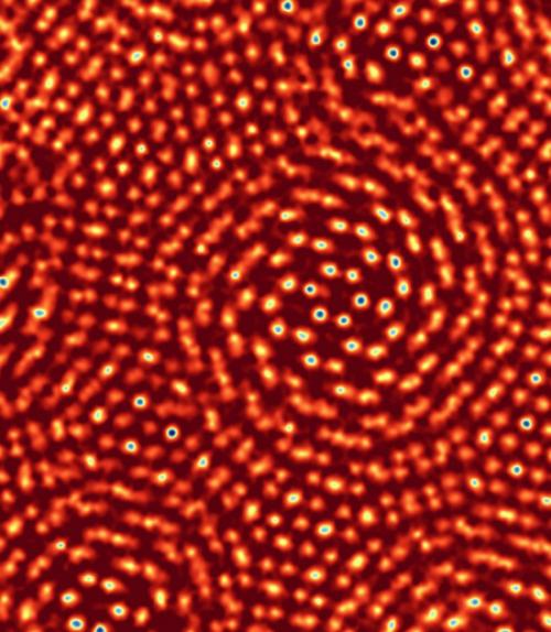
Previous records for resolution were achieved with an aberration-corrected lens and super-high beam energy – 300 kiloelectronvolts (keV) – to obtain sub-ångström resolution. Atomic bonds are generally between 1 and 2 ångströms (Å) long – an ångström is 0.1 nanometers – so sub-ångström resolution would allow one to easily see individual atoms. The Muller group was able to reach a resolution of 0.39 Å – a new world record – and at a lower, less damaging beam energy where resolution from the aberration corrected lenses alone was 0.98 Å.
Muller’s group used the EMPAD and a technique known as ptychography: As the electron beam scans the sample, the detector collects both full-position and momentum distributions of the scattered electrons in overlapping steps. The image is reconstructed from the resulting 4-dimensional data set.
The group used a beam energy of just 80 keV so as not to destroy the MoS2. Despite the low beam energy, the resolution using EMPAD is so good, the microscope is able to detect with startling clarity a missing sulfur atom – “a defect in the lattice,” Gruner said – in a 2D material. “That’s astounding to me,” he said.
With a resolution capability smaller than the smallest atomic bond, a new test object for the EMPAD method was needed. Yimo Han, Ph.D ’18, and Pratiti Deb ’16, from Muller’s group, stacked two sheets of MoS2, one sheet slightly askew, so that atoms from the two sheets were visible at distances ranging from a full bond length apart to lying on top of each other. “It’s essentially the world’s smallest ruler,” Gruner said.
The EMPAD, which has been retrofitted on microscopes across campus, can record a wide range of intensities – from detecting a single electron to intense beams containing hundreds of thousands or even a million electrons.
“The analogy I like to use is, a car is coming at you at night,” Gruner said. “And you’re looking at the lights coming at you, and you’re able to read the license plate between them without being blinded.”
This work was supported by grants from the Kavli Institute at Cornell; the Department of Energy; the Platform for the Accelerated Realization, Analysis and Discovery of Interface Materials (PARADIM), a National Science Foundation-supported platform; the Air Force Office of Scientific Research Multidisciplinary University Research Initiative; and the Cornell Center for Materials Research, a NSF Materials Research Science and Engineering Center.
The MoS2samples were provided by Jiwoong Park, professor of chemistry, University of Chicago; Saien Xie, Ph.D. ’18 (applied and engineering physics); and Hui Gao, doctoral student in chemistry at Cornell.
This story also appeared in the Cornell Chronicle
More News from A&S

‘End of a hopeful era’: Cornell expert reflects on Wilson and Stone legacies
Music

History Center exhibit chronicles excavation at Ithaca’s ‘Freedom Church’
Ithaca history